I recently got really interested in Game Boy console modding. I started watching The Retro Future on Youtube and saw a bunch of his videos of refurbishing and modifying old Game Boys, and I became intrigued. My first Nintendo console of my own was my purple Game Boy Color (that I annoyingly can’t locate). I never had an original Game Boy, but I’ve always had an affinity for the original design, known as the “DMG” model.
I decided that, since I never had a DMG, I should finally buy a crappy one and fix it up. It seemed like a fun project! So I bought two DMGs (that were supposedly “dead” but really weren’t). I figured instead of making a bunch of smaller modded consoles, I should just fix up one console without any modifications for display purposes, and then make one really nice console with all the bells and whistles that I’d like – the main features being an IPS screen and rechargeable batteries. But the more I started adding up costs and thinking about the games I wanted to play, the more I realized that there were a TON of GBC games that I’d really like to play on a nice IPS screen. But the GBC’s form factor isn’t my favorite – mostly due to my large hands. And I didn’t want to have a modded DMG and a modded GBC, especially if the GBC could do everything the DMG could.
But… what if were to purchase a Game Boy Color and disguise it as an original Game Boy? Oh hoh hoh hoh, delightfully devilish, Nick!

Well, after taking the GBC apart, and trying to shove it into a DMG shell, the answer to that was an emphatic “eh, no thanks.”

On a Game Boy Color, there is just one large PCB inside, as compared to the DMG’s two separate boards that slot nicely into the plastic. Most of the ports are basically on the opposite side of where they are on the DMG. I could cut the board in half, and just rewire the broken traces, but that’s pretty difficult and I didn’t really have much exposure to how these things were wired up when I started, and what was important and what could be rewired easily.
Since finishing this project, I’ve found that some others have made pretty nice GBCs-in-DMGs, but that’s another post for another time.
Anyway, the next generation up from the GBC was the Game Boy Advance. I could just modify a GBA or a GBA SP with a nice screen and battery, but I really actually hate how the non-GBA games stick out of the console. I get it, it’s kind of a necessary thing, and backwards compatibility was definitely nice to have back when I was a kid. But I just don’t like the look at all. Then, I stumbled across a few posts from people who put an SP inside a DMG case. The original GBA board was too weirdly shaped to fit inside the DMG case, but the SP was a comparably smaller square shape. With some heavy modifications and additions, people have been able to get their SP inside the DMG case and have a fully functional GBA. Like this guy.

So, looking through a lot of different projects, it seems that there are many different ways people have done this in the past. I saw many people mod the outside shell to accommodate the actual GBA functionality into the console – like adding L and R buttons. That was a non-starter for me. I don’t think I’m good enough at modding cases to make them look nice. I’ve tried before, and I have failed. I’m just not too artistic, or experienced with that kind of thing; or at the very least, I’m way too bothered by minor imperfections when I make projects like this for myself. I wanted to keep the DMG asthetic as close as possible. I’ll make a separate modded GBA later for playing GBA games if I really want it. You can make some really slick GBAs, and those consoles are comparably cheap and abundant anyway. So yeah, GBA compatibility is out. But, I can still use an SP motherboard to play Game Boy Color games.
Therefore, I will be making an original Game Boy that can play up to Game Boy Color games by using a stripped-down Game Boy Advance SP motherboard. There will be no GBA support.
After paging through forum posts, some photo albums, Youtube videos, and lots of schematics, I finally have formulated a plan for how to do achieve this goal. Here are the specifications of my mod:
- An original Game Boy that plays Game Boy and Game Boy Color games
- An IPS screen, with the original screen resolution of the Game Boy/Game Boy Color (160p x 144p), and brightness control via a button that takes the place of the contrast dial
- A rechargeable Li-ion battery, with a capacity of 2000 mAh, that is recharged using the original AC adapter through the DC jack on the side of the Game Boy
- Stereo headphone compatible, with an audio amplifier modification for the speakers
- No external case modifications to the original Game Boy shell (but lots of internal modifications)
(Though… to be completely fair, I will have to clip back part of the power button slider, to allow Game Boy Color games to be placed in the cartridge connector – whether you want to count this as an “external” case mod or not is up to you)
Here’s a bill of materials that I’ll detail throughout the article, and the prices I bought them for (your results may vary):
- Original Game Boy – $30
- Game Boy Advance SP – $50
- Game Boy Advance SP Cartridge Connector – $8
- Custom DMG shell – $15
- DMG glass lens – $3
- IPS Screen and Ribbon Cable (separate items, to make sure the glass lens wasn’t preattached to the screen) – $65
- Common Ground DMG Control Panel PCB – $2ish ($20ish for 10 boards total)
- Custom-made Cartridge Connector Pin Reversal PCB – $1ish ($10ish for 10 boards total)
- Speaker Amplifier Modification Board – $10 (NOTE: unused in final build)
- PJ-320A Headphone Jack – $1
- Two-color LED – $0.50
- 2000 mAh Li-ion Battery – $12.50
- Adafruit LiPo Battery Charger – $7
- eBoot Mini Buck Converter – $1.50
- Momentary Normally-Open Pushbutton – $0.10
- Discrete parts (resistors, transistor), thin wire (28 gauge or smaller), solder, Kapton tape – $??
- Patience – Priceless
The total came out to about $210, not including some shipping and the cost of items I already had lying around. That’s… a decent bit of money. But it’s cheaper than making a modded DMG as well as a modded GBC, and I think this’ll become my defacto Game Boy to play. I don’t think I’ll be making another one of these.
For reference, here’s a schematic for the SP, and here’s one for the DMG. Throughout this post, I’ll be referencing things by their pin numbers, mostly from the DMG board. So I used this reconstructed PCB view of the DMG main motherboard to find the proper numbers. Not coincidentally, the schematic and PCB of the DMG came from forum user bit 9 at chipmusic.org. Thank you mystery internet person! Also, I’ll be using some pictures/views from the Game Boy Hardware Database because I’m bad at taking pictures. Full references can be found on the bottom of the post.
This is not really meant to be a tutorial, as it’s highly customized to the hardware I had available and the systems I was working with. And like I said earlier, it doesn’t include GBA support, like many people probably would be interested in – but I think this is still a good resource to get you most of the way there, or at least provide some background information on the Game Boy line. If you want to follow this guide yourself, you can, but be warned that it’s pretty tight, expensive, and easy to screw up. There are also probably some better methods out there than the way I did. But, I started writing this, and I’m up to like…. *quickly checks*… 10,000 words? Ok yeah, I’m not deleting this. Read at your own peril.
I am not responsible for any damage done to you or your property!
Full disclosure, this mod actually died a few weeks after I finished it up. I isolated the problem to the power supply IC on the SP motherboard – essentially, over the course of the time I played it, the power supply would get weaker and weaker to the point of not being able to boot up at all. I bought this SP used and it had some other issues (that I’ll detail in a bit) so I am suspecting it was always damaged from the start. If I were to do this again, I would get a fully functional SP instead of a partially damaged one – I do not believe there is anything technically wrong with the process (and a few other qualified persons have said as much). So, this post will remain here for posterity, and maybe it’ll help you out if you need it.
Here’s how I did it.
Testing the Hardware
The first thing I did before I started was to make sure everything worked properly. Didn’t want to go knee-deep into the process only to find out that the link port of the DMG I had bought didn’t work for some reason. So, I fired up my copy of Pokemon Red on one Game Boy, and Pokemon Yellow on the other (but not before replacing the battery… RIP my level 100 Pikapal from 1999  ) and connected them with a link cable. I also did checks for all the buttons and volume controls, as well as check the charge port on the SP and the DC jack on the DMG. I connected up the SP’s IPS screen as well, to make sure that all worked.

(This picture was actually a bit later into the process but this is generally what I did anyway.)
There were only two casualties – the DMG’s speaker and the SP’s charge port. The DMG speaker was easy enough, I had an extra one lying around and that seemed to fix the problem fine. The important thing was that it wasn’t the volume potentiometer I wanted to use. I verified that it was working with a multimeter.
The SP’s battery charger not working, now that was a bit more of a bummer. I had expected to just be able to swap the SP battery out with a bigger one. I double checked with another SP, to make sure it wasn’t the battery’s fault, and it charged fine in the other SP. So it was definitely the charging circuit. Fixing this might be easy to do – the fuse might just be blown, and the circuitry could have survived.
Checking the Fuses
First thing to check on an SP, if during testing the main power or the charging doesn’t work, are the fuses, and replace if necessary. You can check to see if a fuse is good by using a multimeter and measuring resistance. If it measures zero ohms (short circuit) that means the fuse is not blown.
F1 is located on the battery charging circuit, and F2 is in-line with main power. They’re located here:


If you find that one of these is blown, do not just solder bridge the pads. If you short the pads to bypass the fuse, and the issue is still on your board, you might let the magic smoke get out! You need to make sure the error is fixed. If you’re going to replace these, you can get replacements like these on Digikey. One common issue that can blow the fuses is shorting something to a place it shouldn’t be shorted to – this won’t necessarily kill the entire board, that’s what the fuses are supposed to protect against!
OoOoOoo do I sense some foreshadowing?
Unfortunately in my case, F1 was fine. So I guess the actual charging circuitry has an issue. No worries, all I needed to do was put an external charger for the battery I wanted to use, nothing too complicated. We’ll get into that later.
Other than those two relatively minor issues, everything seemed to be in working order. So I’ve got two donor consoles now – time to start frankensteining them together.
Preparing the SP Motherboard
One of the most important first steps of the mod was figuring out how to fit the SP board inside the DMG shell. I wasn’t immediately sure how to do this in the most efficient way possible. So to get a good idea of how this is going to fit, I started by taking all the parts off that I wouldn’t be using, or would be replacing.
Some of the pictures throughout this post might show the board with a few parts still present, but saving parts for removal later doesn’t give you any benefit.

L and R Buttons
Let’s start with the low-hanging fruit. As I said for my mod, I won’t be adding L and R buttons to the exterior of the case, to keep it nice and clean on the outside. Off these go! I carefully clipped the pins and then desoldered what was left over.
Game Boy Mode Switch
Near the cartridge slot, there’s a switch that is actuated when a Game Boy or Game Boy Color cartridge is inserted into the SP’s cartridge slot. GBA games don’t hit this switch; that’s what the notch in the side of GBA games is for – to prevent hitting this switch. This switch will tell the SP which mode to run in. Interestingly enough, GB and GBC games run at 5V, whereas GBA games run at 3.3V. So this switch will effectively change the operating voltage of the cartridge slot (and EXT connector), just depending on which game you have inserted. Neat!
Because I’ll only be using this for GB or GBC games, I’ll remove the switch and hard wire it right now to permanently be in 5V mode. Very easy to do, just wire the outside two pins together, and the inside two pins together. Note that the middle two pins ARE tied together in this picture, it’s just hard to see.


Link (EXT 1) Port
Originally, I was afraid there was some kind of weird level translation when communicating between Game Boys and Game Boy Advances, because GBAs run at 3.3V, whereas original Game Boy models run at 5V. This extends to the link cable as well. But, as we saw with the Game Boy Mode Switch, that’s not actually an issue! If you’re playing a Game Boy game on a Game Boy Advance, you’ll be running at 5V. And all the link ports on the Game Boy series share the same pinout. So this’ll be a 1-to-1 wiring. Take it off!
Charging (EXT 2) Port
This is the port specifically for charging the battery, as well as outputting audio to special SP headphones (I didn’t even realize these were a thing until recently). Since I’ll be using the DMG’s DC jack for charging, and the battery charger on-board doesn’t even work anyway, and the audio can be grabbed from elsewhere on the board, this port comes off.

Battery Contact
This one is pretty straightforward too. Taking this off was pretty easy – just heat up the anchor pad, slightly lift it off, then carefully remove the other points by heating the pads up sufficiently. Then, I marked which pad was positive and which was negative, so I don’t accidentally reverse the polarity when wiring up the new battery. If you’re following along at home – I highly recommend doing this so you don’t reverse the polarity of your battery on accident! Since this port just applies the battery to the power supply of the board, you can simply wire up your desired battery instead (even if the charger is broken, like mine).

Power Switch and Volume Slider
These will both have parts from the DMG to use in place, but that just involves adding wires to the correct pads (covered later). Taking these parts off was kind of a pain – hard to heat up the solder on the proper pins to lift it off the board carefully. I then cut the leads with clippers – VERY CAREFULLY – and even then still ended up ripping one of the pads off. Luckily, the pad in question wasn’t crucial for anything, but if you’re going to do it like I did, make sure you’re taking extra care to not stress the pad connections to the board. Maybe use a heat gun.
Cartridge Connector
Just kidding! At this point in the process, I kept the cartridge connector on, in order to continue testing games throughout the build to make sure I didn’t damage anything crucial along the way. Though, eventually this will have to come off.
Preparing the DMG Motherboard
The next step to take was to cut up the DMG motherboard to harvest it for parts! I used my Dremel for this. I tried to keep at least one mounting hole from the PCB so I’d have an easier time lining it up and securing it to the case when I put it all back together. Before cutting it up, I removed parts from the board near the cuts I’d be making, like capacitors, resistors, and diodes. I saved three sections of the board: a portion with the link port and volume dial, a portion with the power switch and DC jack, and the cartridge connector.


After using the Dremel, I cleaned up all the boards with some isopropyl alcohol. I’m hoping to secure the parts to the case by just the screws, but there’s only one hole for each of these segments (besides the cartridge connector) and I imagine I might need to use some glue as well.
In the end, I didn’t actually end up using the cartridge connector slot, because of space reasons, but I’ll explain that later on.
One thing to note, since I’m already talking about Dremeling up this PCB, I needed to isolate the DC jack from the power switch. On the original DMG, the power from the DC jack is wired directly to the power switch, which is bad because I want to charge the batteries with the DC jack, not power the entire Game Boy. So I had to make a cut on the top and the back of the board. The top of the board has a ground plane the whole width of the segment of board, so I had to cut a channel between the switch and DC jack. On the back of the board, there’s a trace that connects the power from the DC jack to the switch.


Oh, and also note, if you’re following this and doing it yourself, do not breathe in dust coming off the PCB when you are using the Dremel. This is fiberglass – not good for your lungs!
With all that yucky PCB cutting out of the way (for now), let’s actually start putting some things inside the DMG shell.
Preparing the Front Half of the DMG Shell
This section will discuss the preparations I made for fitting things inside the front half of the shell. Spoiler alert, it’s gonna hold most of the Game Boy internals, as opposed to the back half. I’ll talk about wiring things later – you might see some pictures of wires in various places, but that’s because I did some testing along the way; for now, this section is just to detail getting everything ready to be wired, to make sure it all fits. Remember that I said earlier that I wouldn’t be doing any external case modifications to my Game Boy. But I will be doing a lot of internal case modding to get everything to fit properly. And it’s gonna look ugly, so don’t bother letting me know that it is. I know. Let’s start with fitting the screen inside the case.
Screen
Because I will be using the innards of an SP in this build, I am going to use a GBA SP IPS screen mod to connect to the motherboard. The external screen lens will be replaced with a glass one, obviously fit for the DMG shell, for maximum durability. Unfortunately, many of the SP IPS screens come with the lens already attached to the screen, and it’s not easy to remove from what I’ve heard. But (last I checked) Retro Game Repair Shop offers the screen separately, so I bought that and a ribbon cable. This made it a bit more expensive, but better than potentially damaging something along the way trying to remove that lens.
(It’s also somewhat annoying that I had to buy parts from multiple different places to get the build I wanted, because they don’t all offer the same stuff, but I guess that’s what I get for doing such a custom build.)
Now, the SP screen is a lot wider than the original Game Boy screen, and mods that utilize the full GBA mode in a DMG shell have to contend with widening the screen area to fit this. But since I’ll be putting this in permanent GBC mode, I don’t have to worry about doing that! I just have to worry about it fitting inside the case. The SP screen is wider than the DMG’s case will physically allow, so I will have to shave off some of the standoffs to get it to fit properly. Not a big deal, all of the shorter ones are mostly there to line up the original DMG screen PCB, no screws to worry about. I just need to make sure it is centered properly.

I also had to shave off part of the base of the four screw standoffs, so that I could wedge the screen in properly.

Looks good, right? Well…

As it turns out, I am Big Dumb. There’s a part of the side of the screen that isn’t actually screen! I was centering it based on the full width of the panel, not by the actual viewing area. This presented a few problems.
The biggest problem was that moving the screen to center it properly meant I had to actually completely remove one of the standoffs that the back of the Game Boy case screws into. Ouch. That almost discouraged me enough to set this aside, but I’m nothing if not stubborn (and also, I’m very prone to the sunk cost fallacy). What I ended up doing instead was creating a 3D-printed bracket that restored the standoff, but allowed the screen to be placed underneath. This had the added benefit of keeping the screen centered properly as well when I secure the screen to the case.

Ok, listen, I know this isn’t the best 3D model out there. I haven’t experimented enough with good 3D modelling software yet, so I’m using the free tool at tinkercad.com. There are a few random cuts/lines all over the place, that’s because I had to reupload the .STL file after the original file got corrupted, and then edit from there. But, it prints out fine and gets the job done. I’m more excited to get this project done than I am excited about finding good easy to use CAD software for my 3D models. If you’re interested in printing this, I have it hosted on Thingiverse.
There are a few features on here that I’ll go into more detail later. The rod shown in the picture, I didn’t actually use in the end. It raised the SP motherboard up too high and made everything harder to fit together. So I just taped down the screen instead.


I used Kapton tape to hold down the ribbon cable flat against the screen. Doing it this way means I didn’t actually have to cut into the left two standoffs, so if you’re going to do it yourself, don’t bother cutting into those! But, I still had to cut into the side of the bottom right to allow the screen/ribbon cable to fit properly. The bracket I printed hugs around the standoffs for extra support. During final assembly, I’ll add glue to keep the bracket secured.
Power LED
If you didn’t notice from the last step, when I shaved off the rim for the power LED, the hole where the power LED sits is completely blocked by the SP screen. There are some modifications out there that completely omit the power LED from the build. I can understand this – you’d have to cut an extra hole somewhere in the case for the power LED, and it wouldn’t have a nice lens over it to cover up the cuts.
But, I really want that LED in there. It just won’t feel right without it. So my plan is to use a surface mount LED in the hole, and drill out some of the case where the screen lens will be covering, and route wires to the LED through there. That’s why there’s a little box coming out of the bottom of the 3D bracket – to allow the LED wires to come through from underneath the screen. The plastic case is about 2 mm thick. You can easily get a small surface mount LED in a 1206 or 1210 package and use thin gauge wires to fit flush with the surface. This is the maximum LED size I think you should go – any bigger, and you’ll be cutting a lot of the shell off, or even be thicker than the shell. The opaque screen lens should block everything out on the front that you shouldn’t see to make it look like the original DMG indicator. Even better – I’ll be using a two-color LED for both the power indicator and the charging indicator (hence the three wires).


I also covered up the wires with some black electrical tape, to prevent any light from bleeding out into the screen or out the sides of the holes. The screen fits nicely on top. This is the LED I used, and here’s a schematic:

Again, I used the red/yellow package. I tied pins 2 and 4 together with the black wire above, because these will connect to GND. The two anodes will go to separate places for the charging indicator and the power indicator.
Brightness Button
I figure this is a good point to talk about the brightness button. The SP doesn’t have a contrast dial like the DMG (well, that is supposed to be easily accessible anyway), but it does have a brightness button. This poses a problem for me… I said no external case modifications! And there isn’t a brightness button or an immediately obvious place for it on the DMG. Have a look at the 3D printed bracket inside the top half of the case again.

If you see there on the right, you’ll see a notch in the case where the DMG contrast dial usually goes. And you should be able to see what I have put near it! On the 3D printed bracket, I added a little holder for a button. This holder was designed to hold this pushbutton in place where the contrast dial used to be. I picked this button because it was the largest button I could find that would fit in this location, as well as having the largest travel distance (how far the button pushes in) of that series. Chosen for maximum satisfaction!

Then, I printed a cover to go on top of the button, so the button actually sticks out and fits flush in the space where the contrast dial used to be. Without this cover, you’d have to jam your finger into the hole, and there’d be some empty space surrounding it.


Great – I’ll be able to add a brightness button without having to cut up the shell! Now, onto the most stressful part of the preparation.
SP Motherboard
The stripped down SP motherboard will sit behind the screen, in the top half of the DMG shell. Placing it with the link port and charging port at the top of the shell seems to fit best. But to do this, I had to make notches in four locations. Two of these were easy. The other two… not so much!
First, the easy ones. The L and R buttons on the top corners aren’t present anymore, and luckily, as it turns out, all the traces on the PCB that are located there just don’t really matter! Cutting off the corners of the board doesn’t cut off access to any other part of the board through a power plane, and obviously we don’t care about the traces going to the buttons since we’re not using them. Just had to be careful not to cut off any other parts.


Now, that takes care of the top two posts. The bottom two posts will require a bit riskier cuts. They’re kind of near the bottom-middle of the board on either side – one near the audio amplifier, and the other by the Game Boy mode switch (which was removed).


Luckily, this only cut into power planes, not any signal traces. I didn’t bother doing anything on the right side of the board, but on the left I get pretty close to cutting off that thick trace, so I ended up soldering a wire from the top of the board to the bottom using some vias just to make sure the connection is still good.
After doing all these cuts, I cleaned them all up really nicely with isopropyl alcohol, and made sure I wasn’t shorting any of the internal planes. This is a four-layer board, so the inner planes should be isolated from each other sufficiently. Luckily, all the cuts came out pretty clean.

With those cuts, the whole thing fits pretty nicely! (Ignore the DMG Control Panel PCB for now, winky face emoji).

Now this far in, I wired in my battery management board and the DMG power switch (don’t worry, we’re getting there) just to test a game with the screen plugged in to make sure a game would still boot up. Luckily, everything seemed to be ok. That’s good, because the next step is to remove the cartridge connector.
*shudder*
This is a crucial point in the mod! After removing this, I won’t be testing again until I have everything pretty much put together. I opted to use a Dremel to cut through the pins. I was surprised by how much I actually need to cut into to get the pins disconnected, but I went very slowly and carefully, making sure nothing gets nicked or bent out of shape. I also cut off the anchor points on the back of the connector, because desoldering them wasn’t working out too well. The whole reason I used a Dremel to disconnect the connector is to reduce the stress on the fragile pads on the SP motherboard. My original plan was to use a heat gun and try to remove it that way, but there are so many tiny parts nearby that I didn’t want to accidentally desolder something else in the process.

There sure was a lot of copper dust after the fact. So before I tested ANYTHING else, I got rid of all that dust using isopropyl alcohol and compressed air (don’t inhale it!).
Afterwards, I removed the rest of the pins using a soldering iron and tweezers. Then I cleaned up the pads with some copper braid to get rid of all the old solder. And here is where I’d put a picture of the board finally stripped all the way down, but I was dumb and forgot to take a picture. Deal with it!

Now that the top portion of the DMG shell and the electronics are ready to go, I’m going to do some small preparations for the back half of the DMG shell, which will house the battery, battery charger, and buck converter board.
Preparing the Back Half of the DMG Shell
Most of the battery compartment is going to be stripped down. You can see in the picture, I first removed all the battery contacts, cut up all the plastic ridges that hold the AA batteries in, and crucially cut a hole in the left side of the compartment for the lithium-ion battery to slot into safely.


Remember that this compartment will have five wires coming out of it that will snake through to the internals of the Game Boy – two coming from the DC jack into the buck converter board, two going from the battery charger that will connect to the SP’s battery terminals, and one going from the battery charging board for the yellow LED. All of the boards in here will be properly protected so nothing short circuits, using Kapton tape. Luckily, everything fits if you orient it right, and the battery compartment still closes!
So now with the cases properly cut up, and the electronics ready to go, let’s start wiring everything together.
Wiring Parts to the SP Motherboard
Here, I’ll go over how to wire up various parts to the SP, and try to be as clear as possible about it. My process for this was to first wire everything up, as detailed below, with decently long wires with plenty of slack, holding various things down with Kapton tape, to make sure I’m not ripping any pads off. It is quite easy to rip pads off if you’re not extremely careful. After I verified the function of everything, I then placed the SP motherboard inside the DMG shell to get a good idea of the placements of the different components, and then replaced the long wires with properly-sized ones. When everything was placed exactly where I wanted it, I used hot glue to secure the wires to the board as a form of strain relief, so I don’t stress any pads when re-assembling the console. Hot glue is non-conductive, easy to apply, pretty strong when applied correctly, and relatively easy to remove if you make a mistake. I tried to keep from adding hot glue on top of solder pads, in case I needed to touch them up or measure them or something else.
A few notes about temperatures! If you are going to heat up a pad or wire near hot glue, you can expect that hot glue to heat up pretty quickly. Also, if you use hot glue on a 3D printed part (PLA plastic, anyway) the plastic will probably melt. Keep it quick! My bracket got kind of melty when I was securing parts.
With that disclaimer out of the way, I’ll start by talking about the thus-far often-mentioned DMG Control Panel PCB.
A, B, D-pad, Start, and Select Buttons
Obviously, the DMG has buttons in much different places than where the GBA SP has them. Luckily, the buttons on a Game Boy are very simple – they just short a line to GND to indicate that the button has been pressed.

There are vias and pads called out all over the board that we can solder wires to to short them ourselves. These will be the “TPxx” numbers you see in the schematic. In the pictures below, you’ll see where I soldered wires. You can see on the silkscreen (the white text on the board) which TP numbers are which. Here’s a list for easy identification, along with wire colors I used and the approximate location in the pictures beneath:
TP0 = A (Blue wire, under the screen connector)
TP1 = B (Yellow wire, under the screen connector)
TP2 = Select (Green wire, on bottom of board)
TP3 = Start (White wire, on bottom of board)
TP4 = Right (Blue wire, under the brightness button)
TP5 = Left (Green wire, under the brightness button)
TP6 = Up (White wire, under the brightness button)
TP7 = Down (Yellow wire, under the brightness button)


These mystery wires will go to the proper locations on the DMG button board that I talked about earlier. This board mimics the input board of the DMG model. Basically, each button has exposed copper traces that are a short distance apart. When the button is pressed, the back of the button rubber pad shorts the two sides together, which then pulls the corresponding pin to GND to indicate a button press. Other than the eight buttons, a ground wire needs to be added as well. I opted to use the bottom exposed ground plane on the other side of the board under the cartridge connector and serial numbers, but there are many other places that are easy to grab. You can use a multimeter to check for continuity with the ground plane.

Note that if you are going to purchase this button PCB yourself, make sure you get the ENIG coating for optimal performance. Stay away from HASL and LF-HASL for this!
Power Switch
Another very crucial part of the build, the DMG power switch is straightforward to connect to the SP motherboard, once you think about it a bit. These two switches are different from each other – the DMG power switch is a DPST-NO/NC switch, and the SP power switch is a simple SPDT switch. What are these abbreviations? Let’s start with the DMG switch. DPST means “double pole single throw.” This means there’s two separate switches that are controlled by a single toggle. NO means normally open, and NC means normally closed. So, a DPST-NO/NC switch has one normally open and one normally closed switch. Here’s a graphical representation of what I mean.

As it is wired on the board, according to the schematic, when in the OFF position, battery power is removed from the main power supplies, and the switch connects the /RESET pin on the processor to GND in order to provide a fast way of killing the game while the power supplies discharge. You can get weird effects if you let a game slowly turn off, including corrupted save data. When the switch is in the ON position, the batteries are just normally connected to the power supply, and the /RESET pin is tied to VCC through an on-board pull-up resistor to allow the game to run normally.
On the SP, the power switch is an SPDT switch, or single pole double throw. This essentially means there is one input that can be connected to two outputs. The power switch will connect the main power supply of the board to the battery when it’s in the ON position, or through a pull-down resistor to GND for fast discharging in the OFF position. In this picture, the switch is turned OFF.

So, it’s luckily very easy to turn the DPST-NO/NC switch into a SPDT switch. All we have to do is connect two of the pins together on one side of the DMG switch, and wire that into our one “input” on the SP board (the power supplies). Just wire it like the following:

(C1 and C2 are just the “C” pin in the SP schematic.)
You can’t tell in the picture very well, but when I cut off the SP power switch, one of the pads kind of came off the board. Luckily, these planes have a lot of places to grab if the pads come off. You can see vias or test points on the planes for each of the pads. So if you screw up like I did, you have backups!
Oh, one note about the power switch. The original DMG switch had a little piece of plastic that extended out to keep the cartridge in during gameplay. It also had the added effect of preventing you from playing anything other than Game Boy games on it. In the picture below, I’m using Game Boy games on the left, Game Boy Color games on the right. And you can see that the button is blocked by the GBC cartridge for the original model.

So I just have to cut off that segment of the switch that pops out when I turn the game on.
So that’s it for the power switch. On the little board I cut up, the DC jack is next to the power switch. So let’s talk about that and the battery charging circuit.
Battery Charging Circuit
Note that if you are following this guide, and your SP battery charger circuit works, you can omit parts of this step, because this battery charger bypasses the one on my SP board that was not functional.
Also note that batteries are very dangerous. KNOW AND FOLLOW PRECAUTIONS BEFORE USING THEM.
The power source has the most electrical modifications necessary for my mod, so this part will be slightly more detailed than others. As I mentioned earlier, my SP motherboard has a non-working charging circuit, but the whole system still works if you give it a charged battery. As I do not want to make any external modifications to the Game Boy, I’m going to use the DC jack to charge my battery. The jack accepts the Game Boy AC adapter. This outputs about 6V nominally. What I want to do is take this 6V and plug it into my battery charger, which will produce the proper voltage/current setpoints for the lithium-ion battery. Adafruit sells a pretty easy-to-use battery charging board, and I figured this was easier/cheaper than making my own board after pricing out the individual parts plus the PCB. Looking at the batteries, I opted to get a nice, beefy 2000 mAh one (with built-in circuit protection!). None of the (larger) batteries that Adafruit sells would fit natively in the battery compartment – but, remember that earlier I detailed the battery compartment modifications to make it all fit.
Note that while I’m assembling things, I always keep the battery unplugged. Don’t want to short anything on the boards accidentally.

I set this board up to charge at a bit less than 200 mA, just to be safe. So from a fully empty battery, it’ll take a bit more than 10 hours to charge up all the way (tests ran after final assembly clock in at approximately 11 hours). I don’t think I’ll care about letting the Game Boy have to sit for a bit longer to charge up, and my instinct is that running this thing at full power should last me 10+ hours as it is (tests ran after final assembly, using a flash cartridge, clock in at approximately 14 hours). To get 200 mA, I soldered a 10kΩ resistor on the “500mA” pad, instead of shorting it. Check out the schematic:

SJ1 there is where I put the 10kΩ resistor. That makes a 12.5kΩ in parallel with a 10kΩ, to give an equivalent resistance of about 5.6kΩ.
Another thing I changed on the board was the charging and charge complete LEDs. The STAT pin on the MCP73831 will pull to LOW logic when the battery is charging, and when it is full, it will instead pull to HIGH logic. That means LED1 is on when charging (red), and LED2 is on when finished (green). In order to keep my two-color LED to use as few wires as possible, I tied the cathodes together, which will be connected to GND. Unfortunately, this means the STAT pin needs to be HIGH logic in order to turn on the LED during the charging period – the opposite of how it normally operates. In order to fix this problem, I simply removed the LEDs from the charging board, and wired in an NPN transistor (2N3904, specifically) to invert the signal, like so:

So, when STAT is HIGH (battery is done charging), the NPN transistor will conduct, and the LED will have both ends tied to GND. But, when STAT is LOW (battery is still charging), the NPN transistor will be off, and power flows from the same voltage on VDD, through the 1kΩ resistor, and through the yellow LED to indicate it is charging. So, there’ll be a wire coming off the LiPo charging board that’s connected to the collector of the NPN transistor, that I will then solder to the yellow LED wire that sits underneath the IPS screen. As for the red power LED, all I need to do there is solder a 1kΩ resistor from the anode to a voltage supply somewhere on the GBA SP motherboard. You can pick either 5V or 3.3V, it doesn’t make a difference.
Ok, now that that’s out of the way, you might be wondering, hey, that text in the battery charger chip’s box says VDD is 3.75V to 6V. And if you look at the datasheet for the MCP73831, the battery charging chip that this board uses, the maximum supply voltage it can handle is 6V. Since the nominal voltage output from the AC adapter is 6V, it’s unacceptable to use it directly. I measured with a meter, and got 6.2V the first time I tried. The regulation on this adapter isn’t tight, and it isn’t meant to be, but we can’t use it without dropping it down a bit first.
In order to handle this varying input voltage, I will be using a buck converter to step down the voltage and keep it at 5V maximum. Again, my original plan was to make this all on one circuit board, but these “eBoot Mini” converters on Amazon come out to only $1.50 each! And they have a tiny footprint too. You can’t beat that.

The only annoying part about this board is that you have to manually adjust the potentiometer to get the correct output voltage, and it’s VERY sensitive. Took me a bit of trial and error to finally get a solid 5V out of it. I used tweezers to adjust the potentiometer.
These buck converters are great for simple stuff, but I think some of the details from the datasheet are dubious. On the datasheet, it says to keep at least 10% load at all time. Buck converters (and many other DC-DC converters) have a discontinuous mode when the load on them isn’t high enough, and this means poor regulation. You can get the output to float too high in this case. Now, if I were to put 10% of the maximum load (3 A) on this thing, that’s a full 300 mA according to the datasheet! With a 5V output, that’s a full 1.5W continuously discharging! So instead, I just slapped a 500Ω resistor across the output terminals. That pulls about 10 mA continuously, or about 50 mW. I checked the voltage with a scope, even without adding that extra load, and the output is still a solid 5V either way. Better safe than sorry though.
So anyway, in summary, I will be using the power from the DC jack on the DMG, at 6V, through a buck converter to regulate to 5V. This 5V will pass to the battery charger, and then to the LiPo battery, which will be connected directly to the battery terminals on the SP motherboard. This way, I can offload charging from the SP to these external boards and effectively replace the damaged charge circuit on the SP, all while not having to add any USB ports to the outside of my case!

Now that we’ve got a very nice block diagram, let’s ruin the illusion with what I’m probably unofficially known to do too often – a terribly drawn schematic in MS Paint. If you’re following this yourself, be careful to use the correct pins for the DC jack and the SP battery terminals. I don’t know if there’s adequate protection against accidentally reversing the polarity on the buck converter board, or on the SP motherboard. I recommend checking with a multimeter that you have the polarities correct before connecting anything up.

And now, explained in text format! On the DC jack, pin 1 connects to GND (white wire), and pin 2 connects to the input voltage on the buck converter (red wire). From the buck converter output, the positive end goes to the 5V hole on the LiPo board, and the GND pin goes to one of the GND holes on the LiPo board. Finally, a GND wire and the Vbat wire from the LiPo board go to the GBA SP motherboard, on the pads where the battery holder used to be. The GND wire goes to the pad closest to the top of the board and the battery voltage wire goes to the bottom pad (the one closer to the cartridge connector). A note that the battery voltage will vary between 4.2V (max charge) and somewhere around 2V if I remember correctly (nearly fully discharged). The nominal voltage is 3.7V, so that’s what I put on the diagram. Also, the USB connector on the LiPo board will go unused (I tried removing it, but was putting way too much heat into the board to justify it).
I will eventually be storing all of this (minus the DC jack, obviously) in the back shell, where the battery compartment used to be. I had to trim out a lot of it to get it to fit. I’ll show this later on.
EXT Port
The other DMG-harvested mini-board that I have house the link port and the volume dial. Let’s knock out the easy one first.
The DMG model’s EXT port is a different size than the Game Boy Pocket, Color, and Advance consoles, but helpfully, the pinout is still the same for each port. As I mentioned earlier, in GBC mode, the GBA SP will operate at 5V, and therefore will be able to communicate with the Game Boy and the Game Boy Color with the right cable. This means I can simply wire the port to the correct pins on the SP motherboard. Easy!
Note that the pin numbering alternates, so one row is 1, 3, and 5, and the other is 2, 4, and 6.

Volume Control
Now, for the fun part. The volume wheel (or slider for the SP) is a simple potentiometer, that is, a variable resistance. Unfortunately, the DMG wheel is a 10kΩ potentiometer, whereas the SP’s volume slider is 30kΩ. Fortunately, the potentiometer on the SP is just used in a voltage divider circuit. It’s a 30kΩ pot (VR2) in series with a 3kΩ resistor (R17). So, if we just change the volume slider to the 10kΩ pot from the DMG, we can change the 3kΩ to a 1kΩ resistor to keep the voltage divider ratio correct, and the result should be the same.

Well, that’s what I initially thought anyway, but then I wired up the potentiometer, and the volume still sounded fine even though it was a lower resistance. I guess the upper end of the volume dial doesn’t actually make the sound much louder? Or, at least, it doesn’t make it noticeably louder. I have no idea how the SP handles it internally. So I figure, why bother risking losing or damaging something while changing the other resistor? Besides, I’ll be adding an audio amplifier to boost the volume of the speaker anyway.
Future Nick here, coming to tell Past Nick to do some due diligence and just try the resistor swap. The DMG volume dial works, but it isn’t ideal. There’s a dead zone for about the first quarter of the dial, and the top saturates pretty quickly. It’s a minor annoyance, but I wish I would’ve tried more things out sooner.
So, here’s the pinouts for the actual dials:

When checking the pinout of the DMG dial myself, I found that there’s an error on the schematic I linked at the beginning of the post. Pins 1 and 2 are simply labeled wrong. I’ve fixed them in the above image.
Unfortunately, since both sides of the DMG dial are tied together at pin 5, we can’t just easily make a 20kΩ potentiometer, so we’ll have to settle with just using one of the pots. On my board, I connected DMG pin 1 to SP pin 1, DMG pin 4 to SP pin 2, and DMG pin 5 to SP pin 3.
Audio Amplifier and Speaker
Instead of just simply wiring the DMG speaker up to where the SP’s speaker terminals are, I included an audio amplifier mod to make the speakers ear-splittingly loud! Seriously… I don’t ever see myself putting this thing up to max volume. The SP’s speaker is smaller than the DMG’s, but they are the same impedance, so the DMG one works fine in place of the SP speaker. This is the audio amplifier board I used. I’m not going to go over how to wire it up, because they already made a guide for that. I followed it and placed the little board in the hole where the speaker used to be.

The two speaker wires (pads shown as the bottom two left pads) go through the hole and behind the main motherboard to reach down to the speaker that will sit beneath the button PCB, where the DMG speaker usually sits. In my opinion, the audio amplifier almost makes the sound too loud, and there’s some background buzzing you can hear at max volume, but it does do what it promises to do.
Headphone Jack
Originally, I was planning on using the DMG headphone jack board and wiring it up to the SP’s board. Unfortunately, it doesn’t work that easily. Some headphone jacks have a switch inside them that gets toggled when headphones are plugged in. That can tell the speakers to turn off, so that you don’t have sound coming out of the speakers AND the headphones.
On the DMG, the headphone jack’s switch for this is normally closed, connecting the pin on the jack to a pin (normally connected to GND) when no headphones are plugged in. When you plug in headphones, that switch opens, so the detection pin is not tied to GND anymore. Unfortunately, this is the opposite to what the GBA SP expects! The SP’s EXT2 port has a pin that is pulled high to 2.5V if no headphones are plugged in. So if we wire up just the DMG headphone jack to the SP motherboard in the way you would expect, with the plug detection switch pin going to the corresponding EXT2 pin, then no sound will come out of the speakers at all because the pin is already shorted to GND by just having the jack. If we plugged headphones in, then the switch opens, and sound would come out of both the speakers and the headphones.
Essentially, we’d need to find an audio jack that is like the DMG, but has the opposite switch functionality (like the SJ-3566AN). But those are difficult to find at a decent price. Following a guide elsewhere online, I opted to buy an external headphone jack – the PJ-320A. I found these on eBay for about a dollar. These audio jacks do not have an internal switch, but if we are using standard headphones with a TRS plug, we can mimic the functionality. Here, you can see the pinout of the headphone jack, and a description of standard audio plugs.

For describing an audio jack or plug, ‘T’ stands for “tip,” ‘R’ stands for “ring,” and ‘S’ stands for “sleeve.” The PJ-320 is a TRRS audio jack. This is important, because plugging in standard headphones with a TRS plug will short the second ring and sleeve of the audio jack through the plug’s longer sleeve. This way, we can create a “switch” through pins 2 and 5 that is normally open when empty, and closed when the plug is inserted into the jack. Wiring it to the SP motherboard is pretty straightforward. Only four wires to worry about. Below are the connections.

The colors here match the colors of the previous diagram. The tip of the plug is the left channel, so the tip pin of the jack should go to the LOUT pad. The first sleeve is the right channel, which should go to the ROUT pad. Easy enough.
Take a look at Q11. If nothing is inserted into EXT2, then the base of Q11 will be pulled to 2.5V through the R42 pull-up resistor, which will pull the net SW to GND. The SW net controls the speaker output – if connected to GND, it will output sound. If the base is pulled to GND instead of 2.5V, however, Q11 will turn off and the speakers will stop making sound. So, we can connect ring 2, or pin 2 of the audio jack, to the base of the transistor Q11 (this also goes to pin 5 of the original EXT2 connector). Finally, wire pin 5 of the audio jack to GND. The mod this was originally based on used the top of C25 for the GND connection, but you can pick anywhere else on the board that’s connected to GND.
So we’ve mimicked an audio plug detection switch – when TRS headphones are plugged in, then pins 2 and 5 of the jack will be connected together, which will tie the base of Q11 to GND, disabling the speakers. An obvious note, but this means this mod will only work for TRS headphones, not TRRS. Luckily, all my headphones that I use have TRS plugs.
There is one more important part to this mod – found by gekkio (thanks for the help!), the creator of the SP schematic I’ve been referencing. The original SP-compatible headphones output sound through LOUT and ROUT, but referenced the headphone speakers to AGND (audio ground) instead of GND. We are not using AGND for the ground of the headphones, we’re using straight GND to get the makeshift headphone detect switch to work (tying the base of Q11 to AGND would not shut off the transistor).
AGND is separated from GND with a 100uF capacitor. This is important, because this capacitor removes the DC component of the audio signal going to the headphones. Because headphones/speakers are essentially coils of wire, their resistance is low, so a DC voltage going through them can overpower them and potentially damage them, depending on the voltage level and the impedance of the coil. Because we need the GND signal to get the speaker disable function to work, we need to add a capacitance in-line with each the LOUT and ROUT channels to remove the DC component. The DMG had this, in fact – two 100uF electrolytic capacitors for each audio channel.

Essentially, our headphone jack needs to be wired like this:

The back DMG shell has a little space for the headphone board to sit, secured with screws – since I won’t have a PCB anymore for this, and the PJ-320A is thinner than the DMG jack, I’ll 3D-print a simple spacer to make the jack fit snugly where the DMG jack used to go. Then I’ll just glue it in, instead of screwing it in. I’m also soldering the wires from the headphone jack to a 4-pin row of header pins. These pins will plug into a socket that’s glued to the DMG button board. This way, assembly and disassembly will be easier, because if I were to glue it directly onto the back shell, I’d have to worry about having the headphone jack connected to wires on the front shell assembly, while being glued to the back shell.


IPS Screen and Brightness Button
The screen install is pretty self-explanatory, and at this point, I’ve done it multiple times for testing purposes. You just need to make sure the ribbon cable is in all the way, in the right orientation, and that the pins on the sides are down all the way to keep it snugly in place. But how do we wire up the brightness button to make sure the screen can change settings?

There’s a solder pad on the right side of the ribbon cable. If we momentarily connect this pad to GND, like, with a push button, the brightness setting will cycle. This is what our brightness button I talked about earlier will go to. All we have to do is take one wire from this pad, wire it to one side of the button, and then wire the other side of the button to GND somewhere on the SP motherboard.
Final Tests, and the Cartridge Connector
At this point, I wanted to make sure that nothing I did so far was obviously screwing anything up. So, I decided to plug the battery into the battery charger board, and make sure the Game Boy would boot up. This allowed me to test everything except the link port, and obviously, the game cartridge connector.

Whew, nothing obviously screwed up. Everything is working just fine. Time to tackle the cartridge connector.
So, if you recall from earlier, I cut off a portion of the DMG motherboard that housed the cartridge connector. I did this because it’s easier to mount this little board, held in by screws, than to glue in a cartridge connector alone into the case. To reconnect the connector, I cut out 32 wires of the same length, a few inches long, and soldered them to the SP motherboard. Then, I soldered those 32 wires, in order, to the DMG cartridge connector board section that I cut out earlier on (at this point I was still thinking of using the DMG connector).

After this picture, I put down hot glue over the wires on the SP motherboard for strain relief. Don’t want to ruin those surface mount pads, as many of them don’t have an easy access point if you rip one off!
I popped in a game, and everything still worked ok! But I had a problem – the cartridge connector was pointing towards the BOTTOM of the console. So I’d have to rotate the connector 180 degrees around to get it to fit. Unfortunately, this didn’t really work – the wires, while long enough to twist properly, wouldn’t be able to be pressed down to screw the whole thing back together (at least, without SEVERELY bending on the SP motherboard). So I instead opted to make a PCB that simply flipped the pinout 180 degrees for me!

Unfortunately, even with this board to reverse the pinout, it still wasn’t enough to fit. The huge bundle of wires was too much – I guess I should have gotten smaller gauge wire. I was using 28 gauge. Oh well. I cut off all the wires near the DMG connector and re-stripped them. I still had this board, but I needed to save space somehow.
As it turns out, the SP cartridge connector sits pretty nicely inside the DMG shell. I had luckily bought a backup just in case. It just needs some securing, because otherwise it’ll wiggle out. So I did what I’ve done to solve every other mechanical issue – 3D print something! This time, a really simple bracket. It just fits around the connector, and slots into the mounting holes around it. I also left space for fitting the PCB. This, along with the 3D printed part, provided great support for the connector. I uploaded it to Thingiverse if you’d like to download it yourself.


You might be able to see in the picture there – the DMG pin spacing is the same as the SP’s pin spacing. Unfortunately since the board was meant to go on a DMG, the pinout is staggered instead of just using surface mount pads. I was able to carefully bend the pins out, and solder them into the board. The board provided some good support for the 3D printed bracket too!
Anyway, I wired everything back up, and it works just as planned. Anxiety levels have abated for now, but this is starting to all come together. So naturally, that anxiety has to start to skyrocket!
At this point, with everything working as it should be, I cleaned up all the wiring. I removed long wires, and replaced them with properly-sized ones where it was needed. I hot glued strain relief in places on the board that didn’t have any components, and made sure to have at least one anchor point for every wire that was soldered to a pad instead of a hole. Then, after everything was wired back up, I redid the tests at the very beginning of the article – traded Pokemon to make sure the link port was working, made sure the headphone jack and speakers were ok, tested all the buttons, and made sure the brightness button worked. Nothing was out of place – it was working as intended. So, now it’s time to start putting everything back together.
Final Reassembly
Unfortunately, at this point, I was getting too excited and didn’t take as many pictures as I should have. But it’s a bit more self-explanatory than earlier steps. The first thing I did was remove all of the electronics from the front half of the DMG. I desoldered the power and charging LED and let the wires hang, while keeping the LED taped securely in the front half of the shell. I also kept the screen bracket in place. I removed the IPS screen from the motherboard (and desoldered the brightness button). I also desoldered the buck converter and the battery charger boards, and let the long wires hang to the side. I’ll be routing these through the bottom half of the shell later.
Now was the moment of truth – removing the protective plastics on the screen lens and the screen itself.
I had been using a plastic lens that I had lying around from another DMG in order to test with, but now it was time to use my glass lens. So I took the plastic one off, and lined up the LED/wires making sure they were in place, secured with the black electrical tape. I peeled off the protector around the edge of the lens, carefully placed the it in, and pressed down. Then, on the inside of the shell, I peeled off the actual screen protective paper with tweezers. No going back now – don’t get any fingerprints on the inside!
The IPS screen came with an adhesive gasket. I cut a portion out where the LED wires would be going under the screen (where the notch in the bracket is located), peeled off one side of the paper to reveal the sticky side, and carefully lined it up inside the bracket. I pressed it down using tweezers. Once that was in place, I peeled off the other side, and got ready to line up the screen. Peeled off that screen protector, and carefully wedged it in underneath the screen bracket corner, making sure to not touch the gasket until it was lined up properly. Pressed down. Snaps into place. Beautiful.

I added Kapton tape to the back of the screen for two reasons. One, the screen is metal, and I didn’t want anything accidentally shorting through it. Secondly, see the holes where I originally had that plastic bar go across? Turns out, that makes the motherboard sit up too high, and makes it harder to close. So I took it out, and instead just used Kapton tape (and a little bit of hot glue) to hold the screen in place. It shouldn’t need too much securing, because the adhesive is holding it in too.
Anyway, after doing all of that, I plugged the screen back into the motherboard, and resoldered the brightness button lead to the ribbon cable. I placed down all the buttons and membranes needed for the button board into their places on the shell, and then carefully placed the SP motherboard and button board back in place, with the speaker in its slot. I screwed in the board, and made sure all the buttons on the front were lined up correctly and felt correct.

Afterwards, I wrapped the bottom and a bit of the top of the link port/volume dial board with Kapton tape – especially around the screw hole where there’s a conductive plane (I poked a hole in it with tweezers). This plane will contact the cartridge slot shield, which will tie the whole thing to ground. Originally, the Game Boy had this as a “radiation shield” like the NES – I think it was just for FCC regulations, or for some minor shielding that isn’t extremely necessary. The Kapton tape will isolate this from the ground connection, making a short less likely. Isolating exposed metal is a theme of this mod! DO IT!
Anyway, I lined it up, and put down a little bit of hot glue to roughly hold it in place for when I actually screw everything back together to properly secure it. Note that the picture below doesn’t show the Kapton tape – I forgot to take a picture of that.

I did the same for the other DMG board segment with the DC jack and the input switch. Then, I placed the brightness button in it’s little holder on the bracket. I had to bend the terminals of this button back a bit, because they get pretty close to the contacts where the mode switch used to be, and also like to get in the way of the 3D printed button. In order to make sure the button lead doesn’t actually contact the board, I added hot glue as an insulating barrier, as well as a way to hold the brightness button in place. I found out quickly that too much hot glue will actually melt PLA plastic… luckily it didn’t do too much damage, and the switch was still secure, but that was a close call.

Next, I wired the power LED to a 1kΩ resistor, and then wired the other end to a 5V power supply. Luckily, the inside two pins on the Game Boy mode switch is connected to the 5V supply! An easy place to grab. So I used that. Then, I glued the resistor down to the button board.

Now I quickly switch to the bottom half of the DMG shell. I mentioned that I printed out a spacer for the headphone jack. Well, I put that in, and covered it in hot glue. This is the only way it’s going to be secured, as the top half of the DMG shell doesn’t actually provide any support for this, so I have to make sure it won’t become loose. After that was ready, I plugged the header pins into the socket I mentioned earlier.

The next part will be to actually close the whole thing up. Before I did this, I went through and looked for all the exposed metal parts that might cause problems when the whole thing is squished together. I added Kapton tape to the pinout swap board, over the exposed metal from the wires going to the SP motherboard, as well as covering up the bottom of the board underneath where the SP connector actually solders to the board. Ok, I think I have mostly everything covered up. Another step I did was adding hot glue between the 3D printed screen bracket and the actual Game Boy shell – particularly around the screw hole in the top right corner. The bracket isn’t actually held onto the DMG shell at all at this point, so we need to make sure it’s secured in order to keep the Game Boy shell halves together!
I placed the bottom half of the shell on top of the top half, and carefully guided the cartridge connector assembly into place. I then placed a game into the cartridge slot to hold the connector in easier, in case something jostled it out of place while I was reassembling. The connector is a pretty tight fit otherwise, no glue necessary, but just a precaution. I threaded through the five wires going to the battery charger and buck converter – two from the battery terminals on the main motherboard, two from the DC jack, and one from the charging LED. Once that was threaded through, I carefully lined up all the DMG board segments, put the brightness button in, put the (modified) power switch, and made sure the wires weren’t getting squished by any of the plastic case standoffs, I put the power button slider in place, and closed it back up. Not too much resistance, luckily.
Then I added screws. There are four on the back, and then two inside the battery compartment. Once those were secure, I resoldered the battery charger and the buck converter to the proper wires, including the charging indicator LED. I wrapped those boards in Kapton tape as well, and placed them in the battery slot.

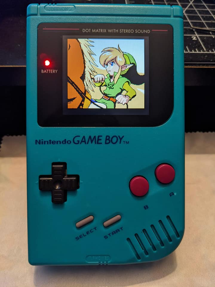
Plugged the battery in, put the battery cover back on, and finally, we have a completed Game Boy. Now let’s just turn it on… and…. wait, nothing is happening. What.
Ok, don’t panic… don’t panic… you can save this. You’ve got this.

Well, I had to unscrew everything and open it back up. I measured between the SP’s power switch terminals (C1/C2) and the pad where the positive battery lead went to on the SP motherboard. This measured an open-circuit. Which means that the fuse was blown. Ok… everything WAS working. What gives?
I scoured the board for exposed metal, maybe it shorted somewhere. And finally, I found it – I had forgotten to completely tape up the DC jack board. There was exposed metal on the back ground pin that shorted the volume dial’s power supply to GND. This caused enough current to blow the surface mount fuse (F2). At least, that’s what I’m pretty sure happened. I taped it up properly, and triple checked for any other possible exposed areas. Then I went to replace the fuse. But.. I don’t have SP fuses lying around.
As it turns out, F1 was still operational. But F1 is used for the battery charging circuit – something I’m not even using, as it’s broken anyway. So I removed F1 in order to replace the blown F2 with it.
Ok… NOW I power it up before reassembling to test. Everything turns on ok. Great, the shorting must have been the issue. Pack it all up, screw it together, place the boards and battery inside the battery compartment, and…. DING. Working perfectly.
Conclusions and Lessons Learned
Well, finally, after months of planning, waiting, modifying, and repairing, this build is complete. I even bought an Everdrive to go along with the build – I might try my hand at some homebrew game development. Unfortunately, as I mentioned earlier, the damaged SP board I was using caused it to fail a few weeks after completing the mod… but I learned a lot about Game Boy architecture along the way, and I’ve got some new confidence for my next mod.
I also learned about some other pitfalls along the way that you should watch out for if you decide to do this mod, or a mod like it.
- This specific mod won’t use the entire screen area of the DMG lens. It’s not a dealbreaker, but part of me wishes I would have gone with a GBC-in-a-DMG mod instead, as those screens are larger. But I hadn’t learned about those until after I was already knee deep in this one.
- Use thin wire. I used 28 gauge, which is pretty small, but still ran into some fitting issues. If I were to do this again, I’d use 30 gauge, at least.
- Hot glue can melt PLA. So be careful using it – don’t put the tip directly on the plastic!
- As I mentioned, the audio amplifier mod (at least the one I got) wasn’t the best option. The sound is loud, for sure, but there’s a lot of white noise in the background. I’ve heard this is inherent to the SP, though, so maybe I should have checked for some dehiss kits or tutorials. With the amplifier removed, I don’t really notice a hissing noise at all.
- Use Kapton tape. Everywhere, if possible. Shielding from any unwanted short circuits is crucial, as I found out!
- New buttons from mod shops don’t necessarily feel the same as the originals. I dunno what it is about them, it almost feels like they aren’t tall enough. I used original buttons to get the feeling as authentic as possible. Your mileage may vary, obviously, but out of the three separate sets of buttons I bought, they all are distinctly different than the original set.
- Don’t trust everything you find online as gospel! That seems obvious to say, but I had a bit of trouble trying to reconcile some information online.
Anyway, I’m really glad I was able to finish this mod up, and I hope this write-up helped you out in some way if you’re planning on doing something like this yourself! Thanks for reading.

References
- DMG schematics: https://gbdev.gg8.se/wiki/articles/DMG_Schematics
- DMG and SP pictures: https://gbhwdb.gekkio.fi/
- SP schematics: https://github.com/Gekkio/gb-schematics/blob/master/AGS-CPU-11/schematic/AGS-CPU-11.pdf
- SP in a DMG mod: http://forums.modretro.com/index.php?threads/infopool-gameboy-advance-sp-inside-dmg-housing.11746/
- Audio amplifier mod instructions: https://handheldlegend.freshdesk.com/support/solutions/articles/67000126349-retrosix-cleanamp-v1-1-game-boy-advance-sp
- Audio potentiometer forum post: https://forums.benheck.com/viewtopic.php?f=22&t=52704
- Headphone jack datasheet: https://p.globalsources.com/IMAGES/PDT/SPEC/431/K1007154431.pdf
- Rechargeable battery mod for DMG (to find the DC Jack pinout): https://www.instructables.com/LiPo-Battery-Mod-for-Your-Gameboy-DMG/
- DMG 01 PCB layout: https://chipmusic.org/forums/topic/13608/dmg-main-board-schematic-circuit-arduinoboy/
- Game Boy cartridge pinout: https://old.pinouts.ru/Game/CartridgeGameBoy_pinout.shtml
- Adafruit LiPo charger schematic: https://cdn-learn.adafruit.com/assets/assets/000/017/043/original/adafruit_products_microlipo.png?1401477385
- DMG button PCB: https://circuit-board.de/forum/index.php/Thread/9847-Common-Ground-DMG-Control-Panel/?pageNo=3&s=5a6c507c679f2a41b528e672daa03713a41902d1
- SP in a DMG video tutorial: https://www.youtube.com/watch?v=h8m8rZbfVm8&ab_channel=andrewmcneil
- Blank DMG circuit board: https://chipmusic.org/forums/topic/13608/dmg-main-board-schematic-circuit-arduinoboy/
- GBdev Discord channel